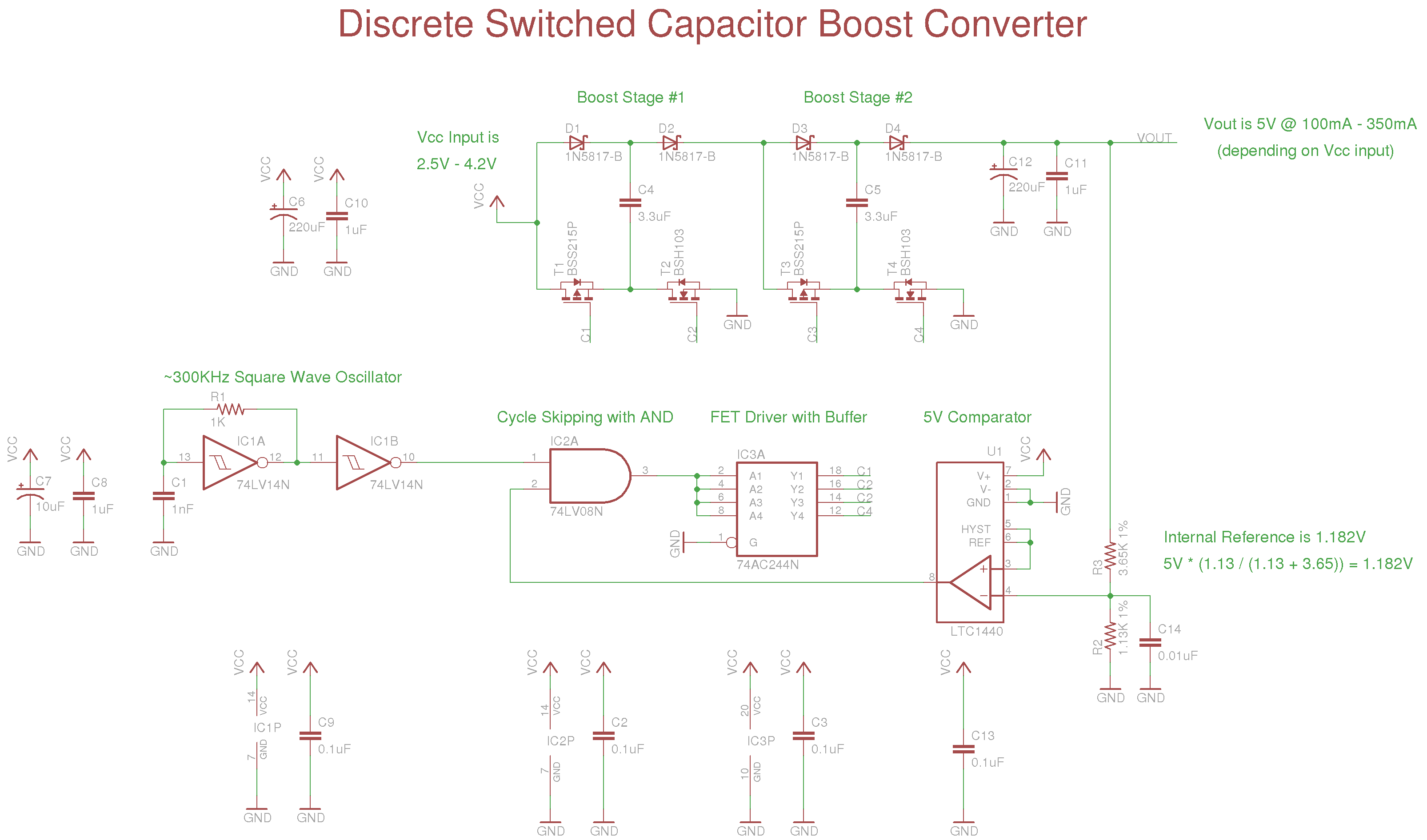
Discrete Switched Capacitor Boost Converter
Theory of Operation

A switched capacitor / charge pump boost converter works by repeatedly charging a flying capacitor to an input voltage source, and then stacking it on top of the input voltage source. This is achieved in the ideal schematic above by alternately closing switch pairs SW1/SW4 and SW3/SW2. When SW1/SW4 are closed, C1 is charged to voltage source V1. When SW3/SW2 are closed, C1 is stacked on top of voltage source V1. After some start up time, the big hold-up capacitor C2 is charged to 2V1, and the load R sees roughly 2V1, provided that it does not pull the charge out of C2 faster than it is replenished.
Design
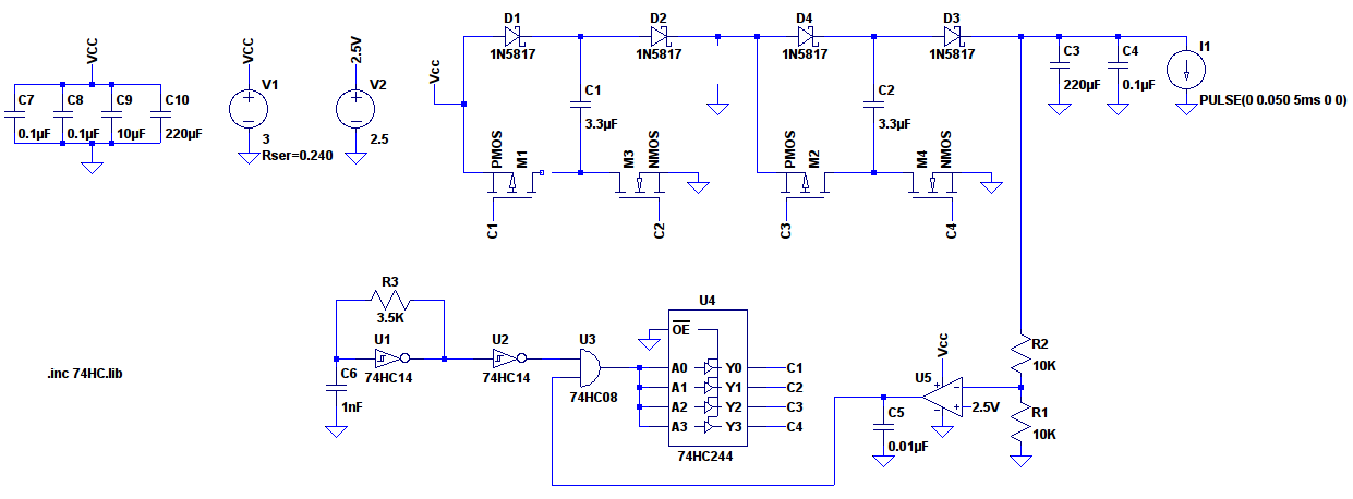
LTspice Schematic: dscbc_ltc.asc
My 5V regulated switched capacitor boost converter consists of two boost stages, a 74x14 based oscillator, and a simple cycle skipping regulation scheme. I implemented the top two switches (SW1/SW2) of each boost stage with Schottky diodes for their relatively low voltage drop, and the bottom two switches (SW3/SW4) with PMOS and NMOS FETs. The diodes work in their switch roles because D1/SW1 will be reverse biased in the discharge/stack phase, and D2/SW2 will generally be reverse biased in the charge phase (unless it is charging the second stage). Since the first and second stages are being operated in phase, the total boosted output is theoretically 3*Vin. The FETs are driven by the 74x244 buffer which has roughly 12mA source / 12mA sink to ensure relatively fast turn on time.
The main oscillator is a simple relaxation oscillator based on the Schmitt-triggered inverter 74x14. It operates at roughly 300KHz. The boost converter regulates the output by comparing a scaled version of the output (Vout/2) to a fixed reference (2.5V) and using an AND gate to disable the clock signal when Vout is greater than or equal to 5V. It therefore skips cycles when the output has reached or is above 5V, and enables cycles when the output droops below 5V.
The voltage ripple and load support of the boost converter depends on the size of the flying capacitors and the load current, because the charge delivered each cycle is proportional to the size of the flying capacitors C1/C2, and the rate that charge is pulled from the large output hold-up capacitor C3 (causing the output voltage to ripple) is the load current. Bigger flying capacitors means greater load support, but also greater voltage ripple for a given load. The voltage ripple and load support are also dependent on the switching frequency, because this is the rate that charge is provided to the large output hold-up capacitor and the load.
I intended my switched capacitor boost converter to be used in a battery application, so I simulated the input source as a 3V source (like two stacked AA 1.5V Alkaline cells), with a worst-case 0.240 ohm series resistance.
Simulations
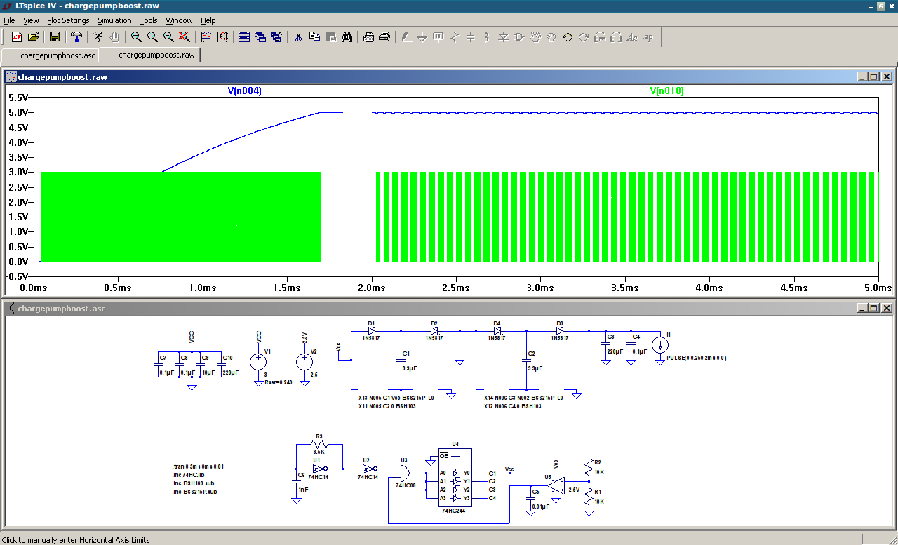
This simulation shows the regulated switched capacitor boost converter operating on a 3V input, creating a 5V output and sustaining a 250mA current source load that kicks in at 2ms. The blue waveform is the output voltage, the green waveform is the switching drive signal. These simulations use the manufacturer’s models for the PMOS and NMOS FETs selected below. The simulated start up time is roughly 1.7ms, though this largely depends on the choice of large output capacitor, as well as the input voltage. The voltage ripple is load dependent: with this 3V input, 250mA load, it is roughly ~20mV. At 300KHz, 3.3uF flying capacitors, and 0.240 ohms output resistance on the input voltage source, the simulations show that the boost converter can sustain up to 350mA with a 3V input, and 100mA with a 2.5V input.
The simulated efficiency is only about 55%. This is likely due to the power loss from the diode’s forward voltage drop, as well as shoot-through during switching transients through the PMOS and NMOS FETs. Changing the diodes switches to all FETs for total synchronous rectification, and delaying the PMOS/NMOS signals to prevent shoot-through would improve efficiency. In addition, a stronger driver than the 74AC244 to turn on the FETs more quickly into their linear regime would also improve efficiency.
Implementation
 |
EAGLE schematic: dscbc.sch
The 74x14 and 74x08 used in the cycle logic was implemented using the 74LV series, which supports supply voltages down to 1V. The 74x244 buffer is a 74AC244 which supports supply voltages down to 2V. The comparator is a neat comparator by Linear Technology, the LTC1440CN8. It features an integrated 1.182V voltage reference that can be tied to one of the comparator terminals for a precise comparison even as the supply voltage droops (which it likely will in a battery application). The LTC1440 supports supply voltages down to 2V. This means that overall this boost converter can operate down to 2V input sources.
The diodes in the boost stages are the 1N5817, as marked in the original schematic. The PMOS is the Infineon BSS215P, and the NMOS is the NXP BSH103. These are small SOT23 surface mount logic-level FETs, chosen for their small gate threshold voltages. The BSS215P has worst case of roughly 200mOhm RDSon, and the BSH103 roughly 400mOhm RDSon for the input voltage range of interest.
I used 3.3uF tantalums for the two flying capacitors, as used in the simulations. The assembled version works well, even slightly better than the simulation, with a matching measured efficiency of approximately 55%.
| Part | Part Used | Digi-key Part Number |
|---|---|---|
74x14 |
74LV14 | 568-2929-5-ND |
74x08 |
74LV08 | 568-2922-5-ND |
74x244 |
SN74AC244 | 296-4311-5-ND |
| Comparator | LTC1440CN8 | LTC1440CN8#PBF-ND |
| Comp. R1/R2 | 1% 1.13K, 3.35K | 1.13KXBK-ND, 3.65KXBK-ND |
| Flying Caps. | 3.3uF Tantalums | 478-1889-ND |
| Diodes | 1N5817 | 1N5817DICT-ND |
| PMOS | BSS215-P | L6327CT-ND |
| NMOS | BSH103 | 568-5013-1-ND |
Pictures
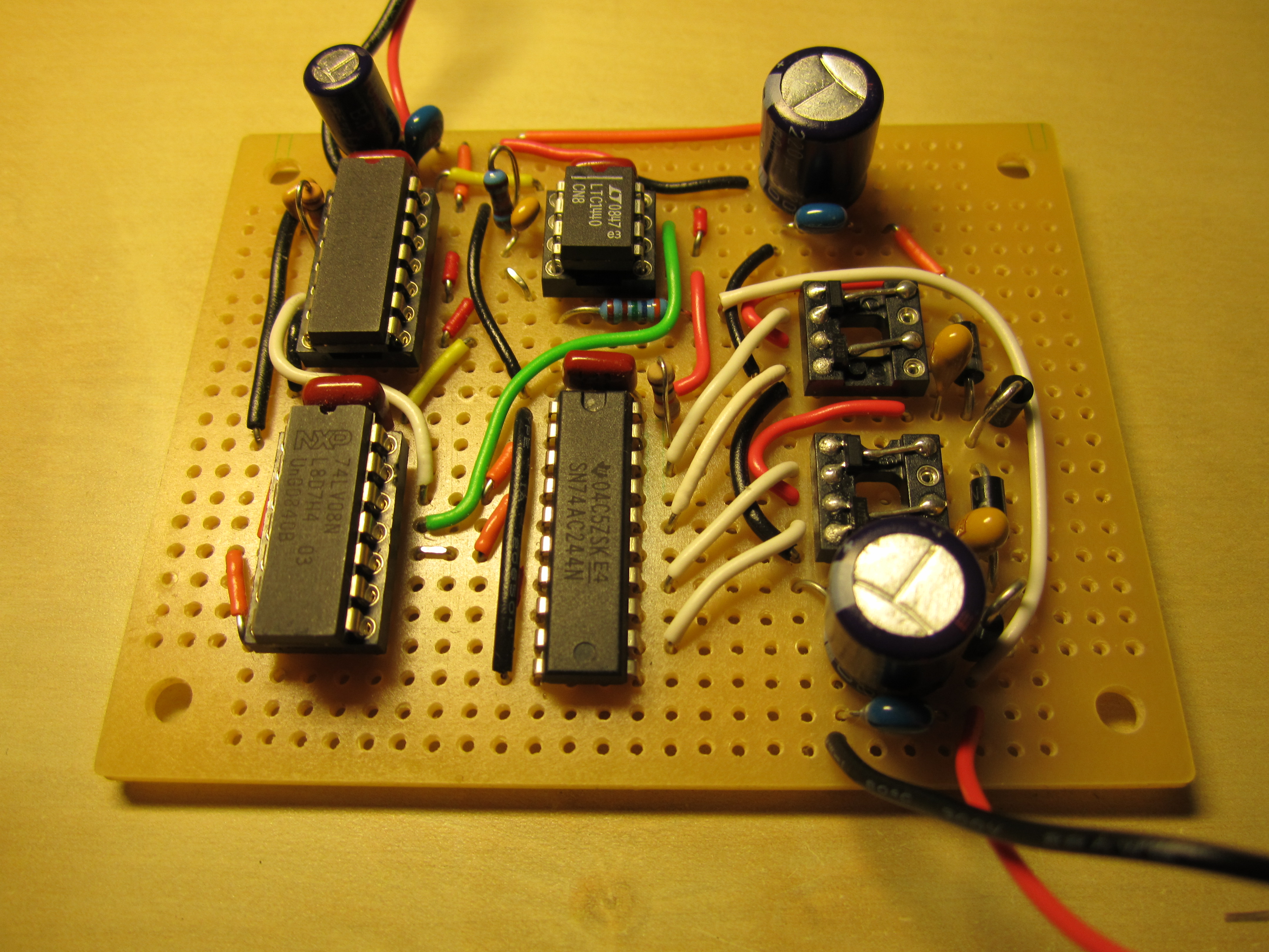
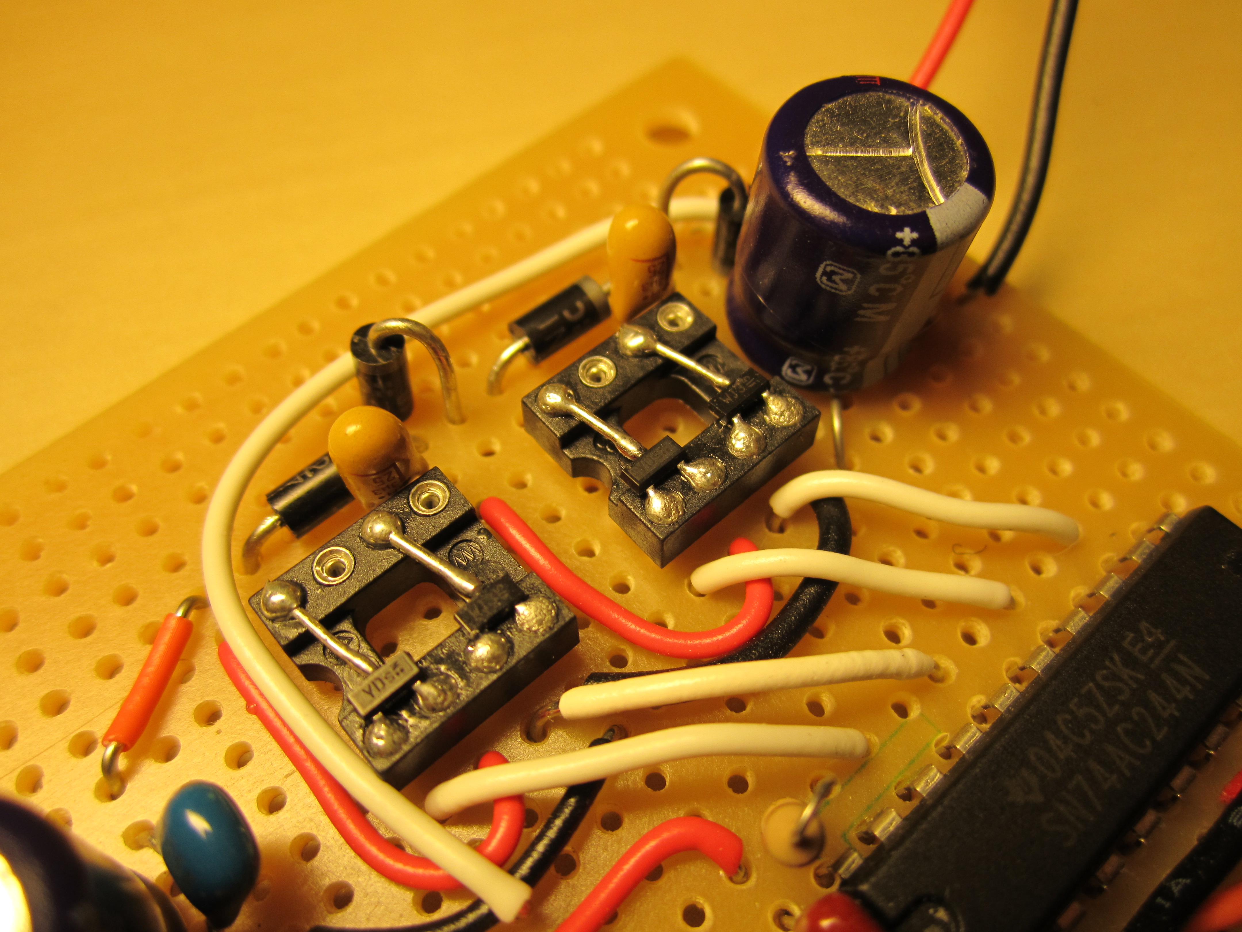
Here is a version of the discrete 5V regulated switched capacitor boost converter I prototyped on a breadboard. From left to right: 74LV14, 74LV08, LTC1440, 74AC244, input decoupling capacitors, FETs and 1N5817s, output decoupling/hold-up capacitors. The SOT23 FETs were soldered to an 8-pin DIP socket.

And the assembled version on a perf. board:
 |
 |
