Interfacing with Parallel SRAM (12/03/2007)
The Cypress CY62256 is a typical parallel-interface SRAM chip. It has a 512x512 array, yielding 262144 bits. Organized in 8-bit words, the capacity is 32768 bytes. Most 8-bit microcontrollers with sufficient I/O are suitable for interfacing with a parallel SRAM chip. I chose an AVR ATMega32.
CY62256 Datasheet: http://download.cypress.com.edgesuite.net/design_resources/datasheets/contents/cy62256_8.pdf
Concept
The pinout of this SRAM chip follows the pattern of most parallel memory chips.
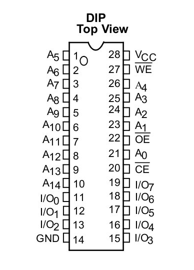
A0-A14: Address lines (15-bit addressing)
Io0-Io7: Data lines (8-bit data bus)
/CE, /OE, /WE: Control lines
Write procedure based on write cycle no. 1 from the CY62256 datasheet:
- Set data port data direction to output (since we’re writing data)
- Make sure the chip is deselected (CE high)
- Put the address on the address bus
- Set WE and OE control lines to high before-hand
- Select the chip (CE low)
- Put the data on the data bus
- Set WE low
- This is when the chip inputs the data
- Set WE high
- End the write cycle by deselecting the chip
Read procedure based on read cycle no. 2 from the CY62256 datasheet:
- Set data port data direction to input (since we’re reading data)
- Make sure the chip is deselected (CE high)
- Put the address on the address bus
- Set WE and OE to high before-hand
- Select the chip (CE low)
- Set OE low
- This is when the chip outputs the data
- Read from the data bus
- Set OE high
- End the write cycle by deselecting the chip
Implementation of the read and write procedures on the ATMega32 running at 16MHz didn’t require delays. Taking into account that each single-cycle instruction takes 1/(16MHz)=62.5ns of time, that the C-code probably won’t compile into perfect assembly even after optimizations, and that the minimum delay required in interfacing the SRAM chip is 70ns (on the slower CY62256-70 version of the chip), the time spent executing the individual control pin toggling instructions serve as sufficient delays where they are needed. Faster microcontrollers/microprocessors may require delays, particularly the time to wait before the data can be read and the time to hold the data on the output lines while it is being written.
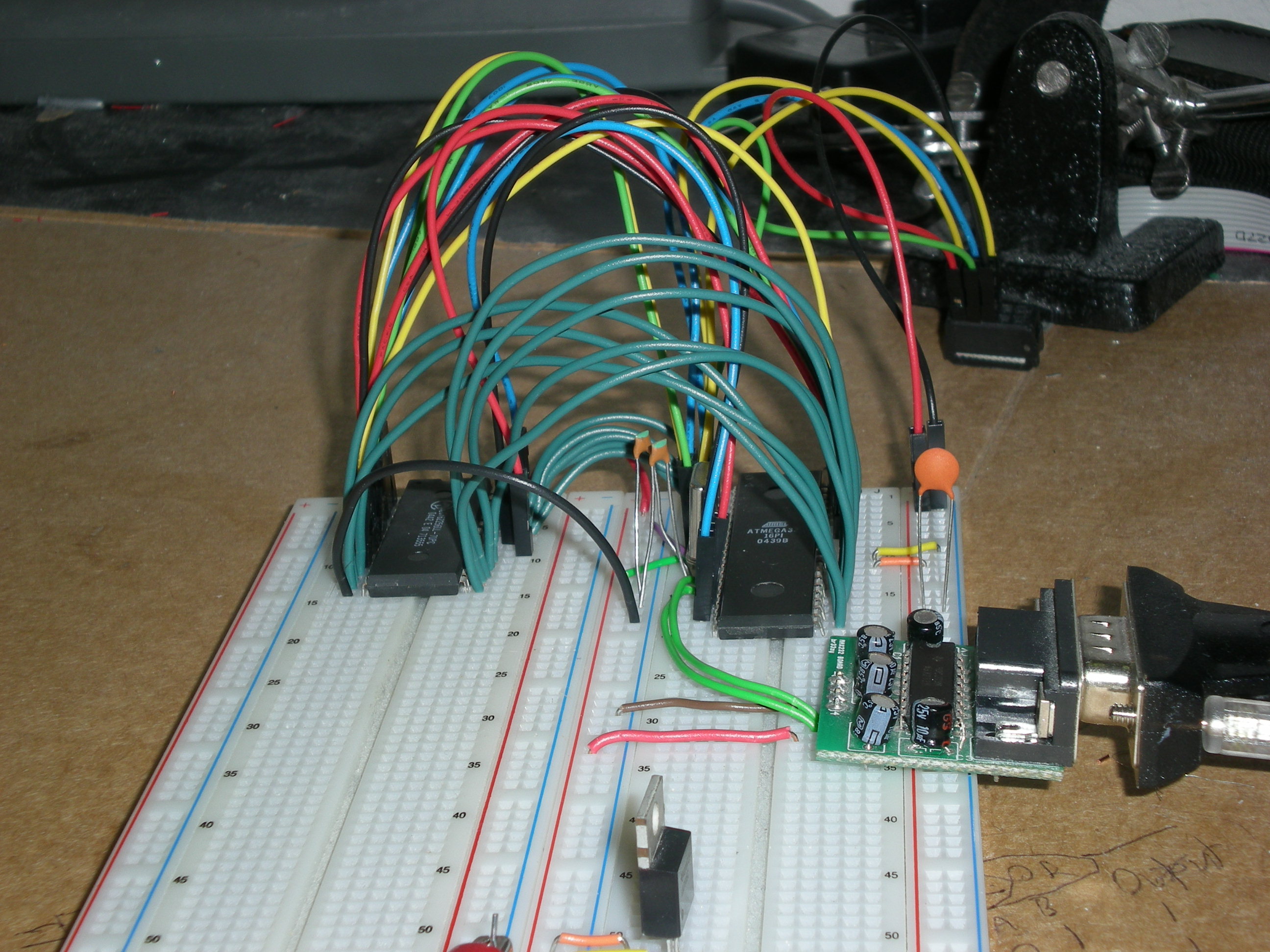
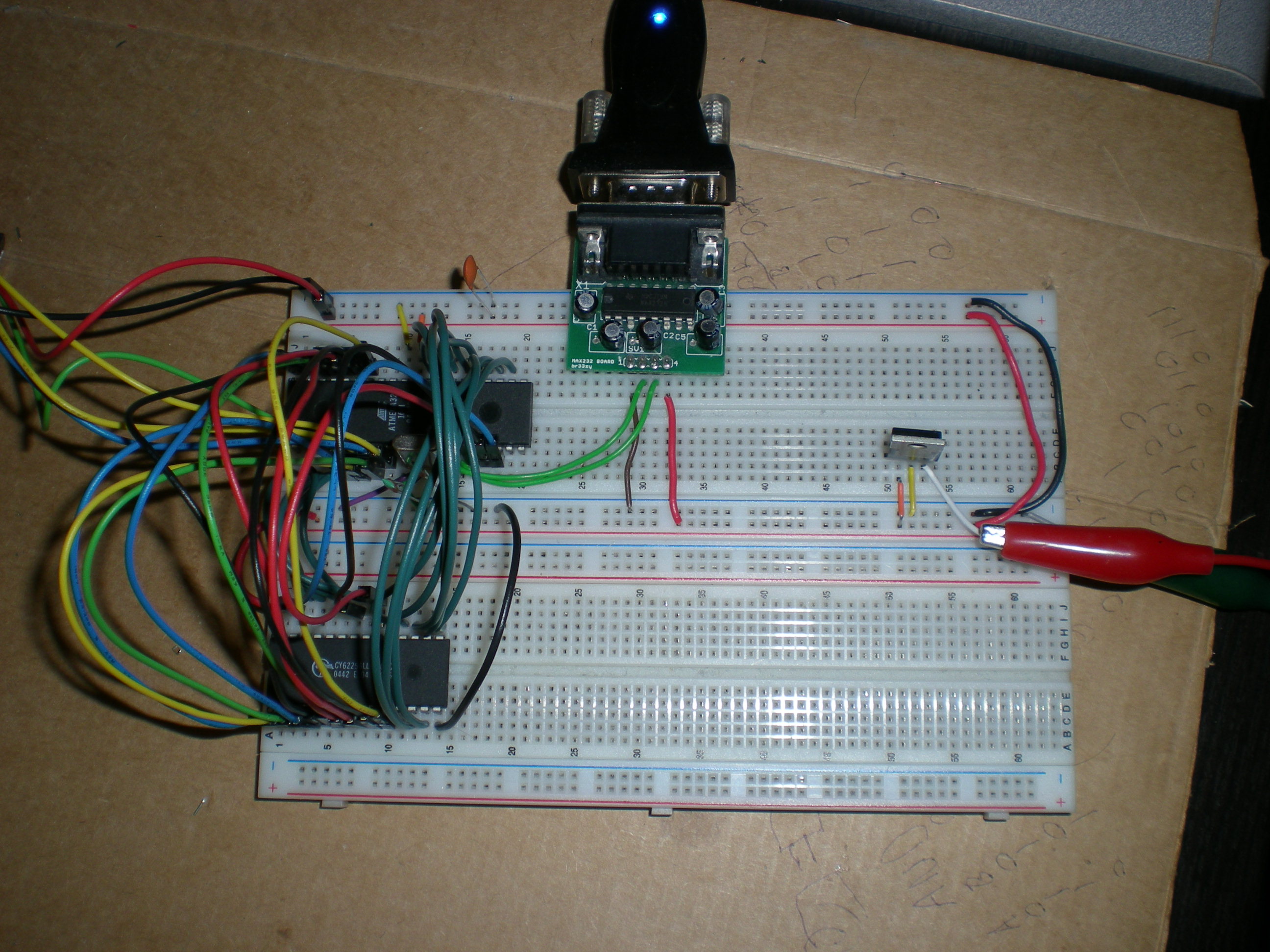
Pictures

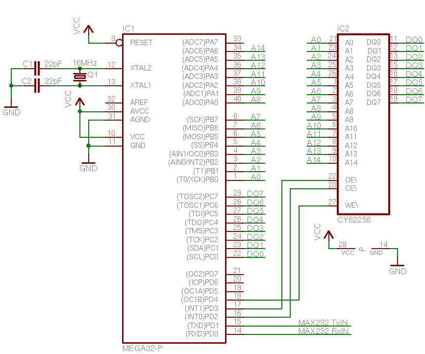
Schematic
Pretty basic schematic.
Source Code
SRAM to ATMega32 connections list:
- A0-A7 to PB0-PB7
- A8-A14 to PA0-PA6
- Io0-Io7 to PC0-PC7
- CE to PD2
- OE to PD3
- WE to PD4
Code, Makefile, and Intel HEX binary are available here: avr-sram-be91938.tar.gz.
